Computer Vision for Circuit Boards: Edge AI Inspection
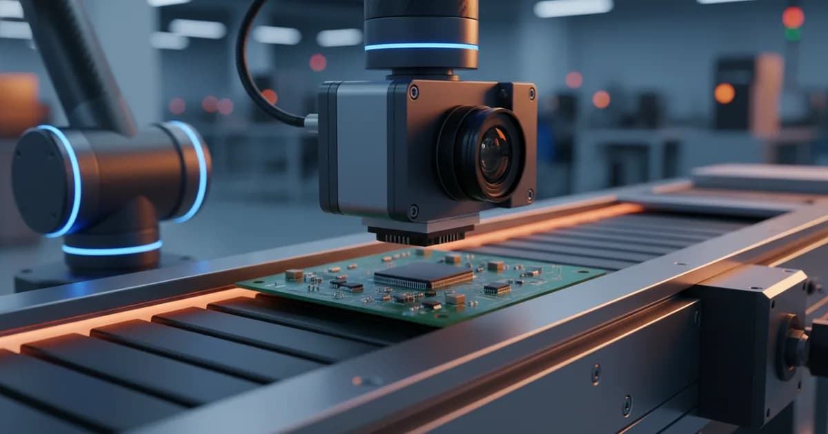
The electronics industry doesn't forgive mistakes. An undetected defect on a motherboard, a capacitor rotated by a few degrees, an insufficient solder joint: that's enough to ruin an entire batch, trigger recalls, and erode reputation built over years. Traditional automated optical inspection (AOI) methods, based on fixed rules and template matching, hold up to a certain production volume — then they break down: high false-positive rates, excessive tuning time, zero adaptability to product variants.
The market has responded with deep learning-based computer vision. Models trained on thousands of real images of circuit boards recognise defect patterns with a precision that rule-based systems can't match — and they do it in real time, directly on the machine. This is no longer experimental technology: companies like Eurotech and their global AOI partners have already deployed edge-native solutions for PCB inspection in high-volume industrial production environments.
Where traditional optical inspection falls short
First-generation AOI systems work by comparison: they capture an image of a component and compare it to a stored golden sample. This works well for stable products with limited variation. In the real world, though, circuit boards change constantly: new layouts, substitute components, lighting variations, surface contaminants. Every change requires manual recalibration that slows down production ramp-up.
The result is a significant false-positive rate that dumps manual-verification work onto operators. The cost isn't just inspectors' time: it's the real risk that an actual defect gets buried in a flood of false alarms. Computer vision based on convolutional neural networks (CNNs) tackles this from the opposite angle: instead of matching against a template, it learns defect characteristics from annotated examples. A model trained on thousands of images of defective PCBs generalises to previously unseen variants, reduces false positives, and maintains sensitivity even on newly introduced products.
How computer vision for circuit boards works
Architecturally, a computer vision system for circuit boards is organised into three functional blocks: image acquisition, model inference, and action.
Acquisition happens with high-resolution industrial cameras. The most advanced solutions use 3D sensors to detect defects such as insufficient solder joints or raised components that escape flat-image vision. Raw data is pre-processed — normalisation, colour correction, possible upscaling — before entering the inference model.
The model is the heart of the system. For defect recognition and classification on PCBs, the YOLO family has dominated applied research: lightweight architectures optimised for real-time inference on embedded hardware. Variants such as YOLOv8-DEE have reached an mAP of 97.5% on the HRIPCB dataset and 98.7% on the DeepPCB dataset. Improved versions using multi-scale detection and pruning techniques have exceeded an mAP0.5 of 99.3% on public benchmark datasets. For applications needing a smaller footprint on embedded hardware, compact YOLOv8 variants maintain accuracy around 95% with significantly lower compute consumption.
The inference output — defect type, location, confidence score — feeds the downstream process: alerting the operator, automatically rejecting the defective component, logging it in production traceability.
Edge AI on the machine: choosing the hardware
Bringing inference directly onto the production line — without relying on a centralised server or the cloud — is the requirement that has driven the rise of dedicated edge AI platforms. The benefits are concrete: minimal latency compatible with real-time rejection on the conveyor, continued operation even without connectivity, and reduced traffic to the data center.
The NVIDIA Jetson Orin family is today the hardware reference point for this kind of deployment. The top-of-range module, Jetson AGX Orin, delivers up to 275 TOPS of AI compute with a 12-core ARM Cortex-A78AE processor and a 2,048-core Ampere GPU — in a compact form factor suited to integration in industrial AOI systems. For applications with lighter requirements, Jetson Orin NX reaches 157 TOPS, and the Jetson Orin Nano Super, priced at $249, offers 67 TOPS: enough for single-camera inspection pipelines with quantized models.
Field deployment follows an established MLOps pipeline: the model is trained offline on GPU servers, converted to an optimised inference format (ONNX, TensorRT), then deployed to the edge device via containers. Incremental updates with new defect data can be pushed via over-the-air updates without stopping production.
Computer vision for WEEE sorting
Computer vision finds a second strategic application area in sorting waste electrical and electronic equipment (WEEE). Automatically classifying incoming components — distinguishing motherboards from power supplies, processors from memory modules, separating materials by type before metal recovery stages — is a prerequisite for maximising the value extracted from WEEE streams.
Systems such as A.R.I.S. (Automated Recycling Identification System), developed in academic research and based on deep learning, tackle the automatic classification of e-waste categories. Architectures such as YOLOv7, trained on electronic-material datasets, have been applied to recognising aluminium, copper, circuit boards, plastics and steel on conveyor belts, paving the way for automating pre-disassembly stages.
Integration with edge AI hardware lets these systems operate in WEEE treatment plants even without cloud infrastructure, with real-time sorting decisions that reduce the need for manual classification and increase the purity of output fractions — a requirement that's become increasingly relevant as European regulations on material-specific recovery rates tighten.
From experimentation to production: what to evaluate
The competitive advantage of computer vision for circuit boards isn't measured only by defects detected: it's measured by adaptability. A model that updates with new defect data is an asset that appreciates over time, unlike fixed rules that age with every product change. Organisations evaluating adoption need to consider three key elements: the quality and quantity of the training dataset (real, annotated defects, not just synthetic images), the choice of edge hardware relative to line throughput, and the MLOps pipeline that ensures the production model reflects emerging defects.
The maturity of edge deployment frameworks — with hardware like Jetson Orin now widely available and proven in production — significantly lowers the entry barrier. Plants that integrate these capabilities over the next twenty-four months will gain a structural advantage in quality, production flexibility and WEEE-stream value compared to those still relying on conventional inspection methods.